Printed Circuit Boards (PCBs) are the foundation of modern electronics. From smartphones and laptops to medical devices and automobiles, almost every electronic product relies on a PCB to function. PCB manufacturing is a complex process that transforms a simple design concept into a fully functional product. Understanding each step of this process—from design to final production—offers valuable insight into how electronic devices come to life.
Introduction to PCB Manufacturing
PCB manufacturing is the process of creating a physical board that connects electronic components using conductive pathways, tracks, or signal traces. These boards serve as the backbone for assembling, testing, and operating electronic circuits. The journey from design to production requires precision, high-quality materials, and advanced technology. Even the smallest error in the process can lead to malfunctioning products.
Step 1: PCB Design and Layout
The journey begins with the design phase. Engineers and designers use specialized software like Altium Designer, Eagle, or KiCad to create the circuit layout.
- Schematic Creation: A schematic diagram is developed to represent how different components are electrically connected.
- Board Layout: The schematic is then transformed into a physical layout that defines the placement of components and routing of copper traces.
- Design Rules Check (DRC): The design is tested against specific manufacturing requirements, ensuring the board can be produced without errors.
This stage is crucial because it sets the foundation for the entire manufacturing process. A well-designed PCB reduces production costs and enhances product reliability.
Step 2: Design Review and Approval
Before manufacturing begins, the design undergoes a thorough review. Engineers check for errors such as overlapping traces, incorrect spacing, or missing connections. Simulation tools are often used to test how the circuit will behave in real-world conditions.
Once approved, the design files are converted into a format known as Gerber files, which contain detailed instructions for manufacturers, including layer information, drill data, and copper trace layouts.
Step 3: Material Selection
The most commonly used material in PCB manufacturing is FR-4, a fiberglass-reinforced epoxy laminate known for its strength and electrical insulation. Depending on the application, other materials like polyimide (for high-temperature resistance) or metal-core substrates (for power electronics) may be used.
Material selection directly impacts the performance, durability, and cost of the PCB, making this step a critical part of the process.
Step 4: Printing the PCB Design
Once materials are ready, the design is transferred onto the copper-clad laminate sheets. This can be done using several methods:
- Photoengraving: A light-sensitive film (photoresist) is applied to the laminate, and UV light is used to transfer the design pattern.
- Laser Direct Imaging (LDI): A more precise method where lasers etch the design directly onto the surface.
The goal is to create a clear blueprint of copper traces that will guide the electrical flow across the board.
Step 5: Etching the Copper Layers
After the design is printed, unwanted copper is removed through an etching process. The most common method uses a chemical solution such as ferric chloride or ammonium persulfate.
This process ensures that only the copper traces required for the circuit remain on the board. For multilayer boards, this process is repeated for each layer, and layers are carefully aligned.
Step 6: Drilling Holes
Holes are drilled into the board to create spaces for component leads and vias (vertical interconnections between layers). Modern PCB manufacturing uses CNC drilling machines or laser drills for extreme accuracy.
The diameter of these holes can be as small as a few microns, depending on the complexity of the design.
Step 7: Plating and Copper Deposition
To make the drilled holes conductive, they are plated with copper. This step ensures that electrical connections between different layers are established.
- Electroless Plating: Deposits a thin copper layer inside the holes.
- Electroplating: Thickens the copper to ensure durability and reliability.
This step is particularly important for multilayer boards, where vias must carry signals across multiple layers.
Step 8: Applying the Solder Mask
After plating, a solder mask is applied. This is the green (or sometimes red, blue, or black) protective layer that covers the copper traces.
The solder mask serves multiple purposes:
- Prevents accidental solder bridges between closely spaced traces.
- Protects copper from oxidation and evironmental damage.
- Gives the PCB its characteristic color.
Step 9: Silkscreen Printing
The silkscreen layer is applied to display important information such as component labels, pin numbers, test points, and company branding. White is the most common color used, but other colors are available.
This layer helps technicians during assembly, testing, and repair.
Step 10: Surface Finishing
To prepare the board for component assembly, a surface finish is applied to exposed copper areas. Common finishes include:
- HASL (Hot Air Solder Leveling): A cost-effective option.
- ENIG (Electroless Nickel Immersion Gold): Provides excellent corrosion resistance and durability.
- OSP (Organic Solderability Preservatives): Environmentally friendly and low-cost.
The finish ensures good solderability and protects the copper pads.
Step 11: Electrical Testing
Before moving to assembly, the PCB undergoes rigorous electrical testing. This ensures that there are no open circuits, shorts, or misrouted connections.
- Flying Probe Test: Uses moving probes to test individual nets.
- Bed of Nails Test: Uses a fixture with multiple probes to test the entire board at once.
Testing guarantees that the board functions exactly as intended.
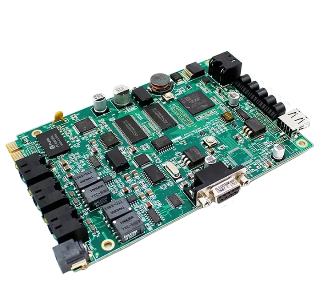
Step 12: PCB Assembly (PCBA)
Once the bare PCB passes inspection, components are mounted onto it. This process is known as PCB Assembly (PCBA) and includes:
- SMT (Surface Mount Technology): Components are placed directly onto the board’s surface.
- THT (Through-Hole Technology): Components are inserted into drilled holes and soldered.
Soldering is typically done using reflow ovens for SMT or wave soldering for THT.
Step 13: Final Inspection and Quality Control
Quality control is critical in PCB manufacturing. Boards are inspected visually and tested using automated optical inspection (AOI) systems, X-ray machines, and functional testing methods.
Any defective boards are either repaired or discarded, depending on the issue. Manufacturers follow international standards such as IPC to ensure quality.
Step 14: Packaging and Delivery
After passing all tests, the final PCBs are cleaned, packaged, and prepared for shipment. Anti-static packaging is often used to protect sensitive electronics during transit.
The boards are then delivered to clients, ready to be integrated into their electronic products.
Importance of Precision in PCB Manufacturing
PCB manufacturing is a field where precision matters. A single error can cause device malfunction, reduced performance, or even safety risks. With increasing demand for smaller, faster, and more reliable devices, manufacturers are investing in automation, robotics, and advanced materials to push the limits of PCB technology.
Conclusion
PCB manufacturing is a fascinating process that bridges design innovation and technological precision. From the initial schematic to the final assembled product, every step requires accuracy and expertise. Understanding this process helps us appreciate the complexity behind the electronic devices we use daily.
As technology advances, PCB manufacturing will continue to evolve—embracing new materials, higher density designs, and eco-friendly practices. Ultimately, the journey from design to final production showcases the incredible synergy between engineering creativity and industrial manufacturing.